Tiếng Việt
Table of Contents
In today’s global semiconductor industry, compliance with international standards such as JEDEC, AEC-Q100, or IEC 61000-4-2 is not just a checkbox—it’s a prerequisite for product acceptance across major markets. For every integrated circuit (IC), Electrostatic Discharge (ESD) and Latch-Up testing play a pivotal role in ensuring reliability, preventing field failures, and enabling global certification.
Understanding the Risk: ESD and Latch-Up Are Not Optional
Throughout the lifecycle of an IC—from wafer fabrication to packaging, handling, assembly, and end-use—electrostatic discharge events can occur at any moment. A single nanosecond-level surge may be enough to permanently damage transistor gates, destroy oxide layers, or cause latent defects that fail later in the field.
Under JEDEC JESD22-A114, a minimum of 2kV HBM (Human Body Model) immunity is required for commercial-grade ICs. For high-performance devices with dense I/O or critical applications (automotive, aerospace, medical), the threshold is even more stringent.
Comparing ESD Models: HBM vs MM
Human Body Model (HBM)
Simulates ESD from human handling (~100pF, 1.5kΩ), relevant in manual operations or assembly environments.
Machine Model (MM)
Represents discharge from manufacturing equipment. MM events typically have faster rise times and can inflict more severe damage.
Both tests are mandatory in major international qualification standards. Failure to pass either model results in rejection from qualified supply chains.
Latch-Up – The Silent Killer in CMOS Design
Latch-up occurs when parasitic thyristor structures are inadvertently triggered, causing a low-impedance path between power and ground. If undetected, latch-up can:
- Instantly destroy the IC due to thermal overload
- Trigger runaway currents, leading to electrical overstress
- Cause critical functional loss in analog or mixed-signal domains
As a result, Latch-Up testing is performed alongside ESD in nearly all qualification flows.
Latch-Up Testing: JESD78 Compliance
JEDEC JESD78 defines standard procedures for evaluating latch-up immunity, including:
- Current injection into I/O pins
- Over-voltage stress on power supplies
- Functional verification after stress to confirm recovery
To pass, an IC must not trigger latch-up under any defined test condition and must return to normal functionality without degradation.
Why This Matters to Semiconductor Companies
Certification Barrier
Failing ESD or latch-up tests disqualifies a device from being accepted in regulated markets (e.g., automotive, medical, aerospace, defense).
Production Yield Protection
Early detection eliminates weak designs, prevents field returns, and reduces RMAs or in-warranty claims.
Reputation & Customer Trust
A single failure in the field can damage supplier credibility—especially in safety-critical industries.
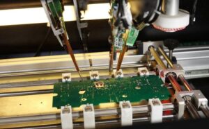
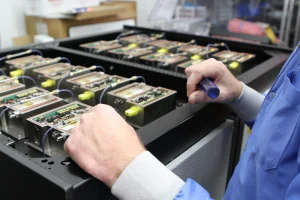
VNST’s Capability in ESD & Latch-Up Testing
At VNST, ESD and latch-up testing are an integral part of our turnkey IC testing services. We provide:
- Full compliance with HBM up to ±8kV, per JESD22-A114
- MM testing capability for machine-related discharge
- Automated Latch-Up testing per JESD78 across all I/O domains
- Fault isolation and failure analysis in case of anomalies
All tests are executed under rigorous QA protocols, supported with industry-standard reporting for qualification submissions.
Conclusion
In semiconductor validation, where a single oversight can cost millions in recalls or failures, ESD and latch-up testing are not optional—they are mission-critical. These tests are not just procedures; they are proof of product integrity, design maturity, and global readiness.
At VNST, we view ESD and latch-up validation as a foundation for market success. With industry expertise, certified tools, and precision testing processes, we help your ICs pass the toughest international barriers—with confidence.