Tiếng Việt
Table of Contents
In the semiconductor industry, where reliability demands are increasingly stringent, especially in fields like automotive, medical devices, aerospace, and industrial equipment, Burn-in Testing plays a critical role in eliminating faulty devices early and confirming the long-term operational durability of ICs.
Burn-in is not just an additional testing step but has become a mandatory part of the quality assessment chain for many major OEMs, particularly for products meeting AEC-Q100 or MIL-STD standards.
What is Burn-in Testing?
Burn-in is the process of operating an IC under conditions of higher-than-nominal voltage and temperature for a specified period (usually from 24 hours to 168 hours) to accelerate potential aging mechanisms (failure acceleration).
The main objectives are to:
- Detect and eliminate ICs that may fail early (infant mortality)
- Test the stability of components under harsh conditions
- Confirm the durability of internal connections (bonding, metallization, oxide, etc.)
Why is Burn-in an Essential Testing Step?
According to the bathtub curve of reliability, most IC failures occur during the initial phase (“infant mortality”). Burn-in helps to:
- Increase usable yield: removing potential faulty ICs before shipment
- Reduce RMA (Return Material Authorization): minimizing post-sale warranty claims
- Meet requirements from large customers: many corporations require burn-in as a prerequisite for accepting devices in the supply chain
Key Parameters in Burn-in Test
| Parameter | Purpose | Common Range |
| Temperature | Activates aging mechanisms | 125°C – 150°C |
| Voltage | Accelerates failure due to stress | 1.1x – 1.5x VDD |
| Pulse Frequency | Simulates real-world operation | Based on application profile |
| Test Duration | Ensures wide coverage | 48 – 168 hours |
Burn-in System: Classification and Implementation
- Dynamic Burn-in
IC is logic-activated throughout the burn-in process. This is applied to microcontrollers, ASICs, SoCs, DRAM, etc. The results reflect real-world operating conditions. - Static Burn-in
IC is subjected to a fixed voltage bias without clock or logic activity. Typically used for analog ICs, memory, etc.
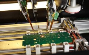
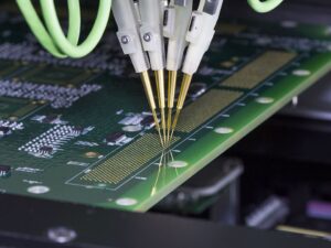
Burn-in Board (BIB) Design
The design of the burn-in board is crucial in maintaining accurate electrical and thermal conditions for each type of IC. Key factors to optimize include:
- High-temperature resistant materials (FR4 TG high, polyimide)
- Short routing, avoiding cross-talk
- Socket and load design that fits the IC’s footprint and power dissipation
How VNST Implements Burn-in Testing
At VNST, the burn-in service is carried out using specialized equipment:
- High-temperature oven (HTOV) capable of precise temperature control with ±2°C uniformity
- In-house designed Burn-in Load Board tailored to specific IC families
- Burn-in socket compatible with various packages: BGA, QFP, QFN, CSP, etc.
- Integration of real-time current/voltage monitoring and test result logging for post-analysis
When Should a Business Apply Burn-in?
| Product Context | Should Burn-in be Applied? |
| Automotive Products (AEC-Q100) | Mandatory |
| ICs with High Transistor Density | Recommended |
| Initial Production Batches (Pilot Run) | Recommended |
| Products Requiring MTBF > 100k Hours | Should Apply |
Conclusion
In IC testing, burn-in is not just a test—it is an investment in reliability. While the initial costs may slightly increase, the benefits include minimizing risks in the supply chain and avoiding irreparable damage when ICs fail after reaching customers.
VNST is ready to assist businesses in designing, implementing, and optimizing the burn-in process to improve reliability, enhance quality standards, and meet international requirements in IC manufacturing.