
 Tiếng Việt
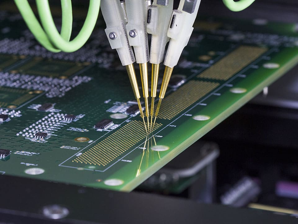
Understanding customer specifications, IC package details, and testing requirements to ensure a tailored Load Board solution.
VNST delivers high-performance Load Board solutions, combining advanced engineering and cutting-edge technology to ensure accuracy, reliability, and efficiency in semiconductor testing.
VNST provides optimized Load Board design and manufacturing, integrating advanced technology and expert engineering for superior quality and performance
Giải pháp kiểm thử và thiết kế với chi phí tối ưu, đảm bảo giá trị cao nhất cho khách hàng.
Tùy chỉnh giải pháp để đáp ứng chính xác nhu cầu của từng khách hàng.
Kiểm thử tốc độ cao đến 10 Gbps, song song trên 128 pin, và điện áp cao đến 2000V.
Thời gian thực hiện nhanh chóng, giúp rút ngắn chu kỳ phát triển sản phẩm.
VNST follows a professional Load Board design and manufacturing process, ensuring precision, quality, and optimal performance for every product.
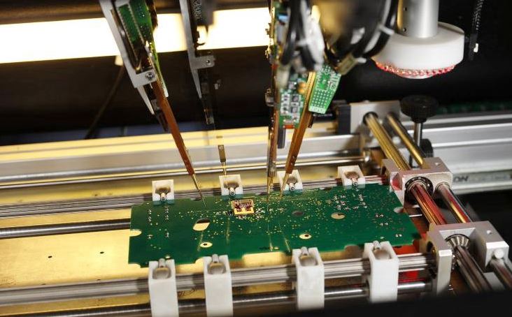
Understanding customer specifications, IC package details, and testing requirements to ensure a tailored Load Board solution.
Developing schematics, PCB layouts, and signal integrity simulations using advanced design tools to optimize performance.
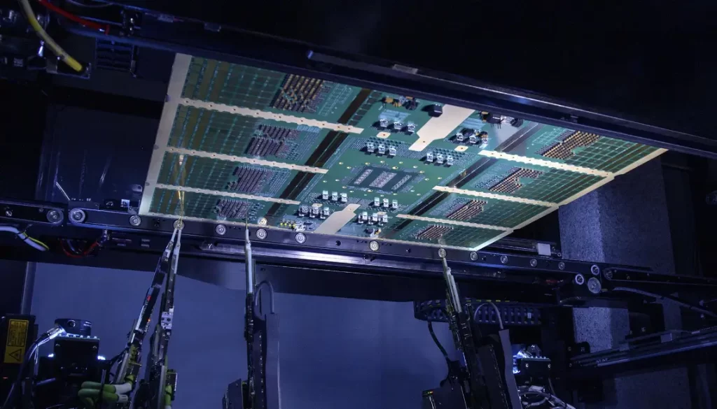
Producing high-density, multi-layer PCBs with precise fabrication techniques, ensuring reliability and durability.
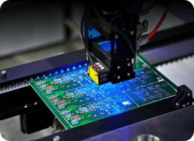
Conducting electrical testing, impedance verification, and final validation to guarantee compliance with industry standards.

A structured test method that sequences data through flip-flops, enabling efficient fault detection and validation of internal logic paths.
Learn more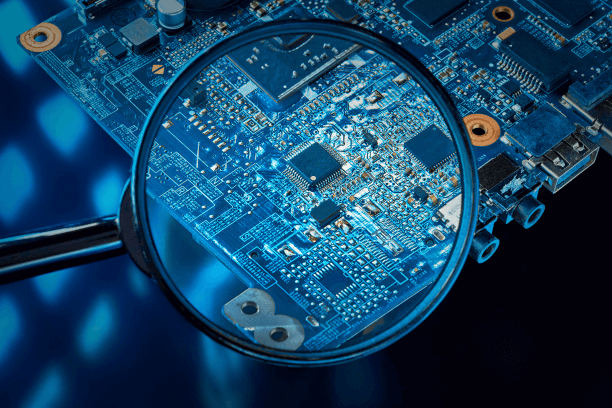
An embedded testing mechanism that allows ICs to self-diagnose functional and structural defects, reducing external test dependency and improving efficiency.
Learn more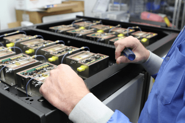
A stress test that exposes ICs to high temperature and voltage to detect early-life failures, ensuring long-term reliability and stability.
Learn more
A systematic approach to identifying defects in ICs, utilizing advanced techniques like SEM and thermal imaging for precise fault localization.
Learn more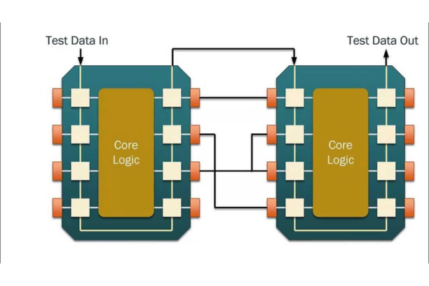
A non-intrusive test method for digital ICs, detecting faults without pin access. Essential for BGAs, ensuring full coverage and efficient debugging.
Learn more
VNST has become a key strategic partner, ensuring the quality and reliability of our FPGA products before they reach customers in the US and Europe.
VNST has become a key strategic partner, ensuring the quality and reliability of our FPGA products before they reach customers in the US and Europe.