Tiếng Việt
Table of Contents
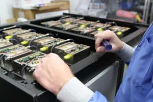
In the semiconductor industry, where each integrated circuit (IC) can contain billions of transistors, ensuring quality and performance is not just a requirement—it’s a survival imperative. IC testing is not merely a final step in production; it is a strategic safeguard that minimizes risk, reduces cost, and preserves brand integrity. Below is a comprehensive overview of widely adopted IC testing methodologies that play a critical role across the modern semiconductor value chain.
Functional Testing
Objective:
Verify the logic behavior of an IC against its design specifications, detecting functional faults or logic design issues.
Key Techniques:
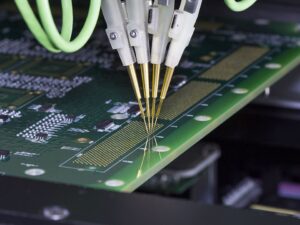
- Scan-based Testing / ATPG: Design for Test (DFT) methodologies insert scan chains into the circuit for internal flip-flop observability and controllability. Automatic Test Pattern Generation (ATPG) algorithms then generate test vectors that maximize fault coverage while minimizing test time.
- Boundary Scan (IEEE 1149.1): Allows non-intrusive testing of I/O connectivity within or between ICs on a board, especially effective for BGA and LGA packages where direct probe access is impractical.
- Built-in Self-Test (BIST): An embedded logic block generates and evaluates test results autonomously within the IC, enabling self-diagnosis. BIST is widely used in memory, analog, and complex logic ICs.
- Functional Pattern Execution on ATE: RTL or gate-level simulations are translated into ATE-compatible test patterns (e.g., STIL to V93K) for real-time validation on Automated Test Equipment.
Parametric Testing
Objective:
Characterize electrical parameters such as leakage current, threshold voltage, delay, and impedance, identifying process-induced deviations and out-of-spec behavior.
Key Techniques:
- Leakage Current Testing (Ioff): Measures off-state current at logic gates, critical for low-power and deep-submicron CMOS devices.
- Threshold Voltage (Vth) Extraction: Utilizes curve tracing to determine transistor turn-on voltage, a key metric for process monitoring and corner analysis.
- Signal Integrity (SI) Analysis: Employs Eye Diagrams to evaluate jitter, distortion, and ringing at high frequencies (> GHz), ensuring robust data transmission.
- Power Integrity & IR-Drop Analysis: Verifies voltage delivery uniformity and detects voltage drops in core domains caused by insufficient power grid design or decoupling strategies.
Reliability Testing
Objective:
Predict product lifetime and uncover latent failure mechanisms by simulating accelerated aging and harsh operating conditions.
Key Techniques:
- HTRB (High Temperature Reverse Bias): Applies reverse bias under elevated temperatures (>125°C) to accelerate degradation, targeting NMOS stress pathways.
- HAST (Highly Accelerated Stress Test): Exposes the device to high humidity and temperature (e.g., 130°C, 85% RH), identifying bond delamination, corrosion, and moisture ingress.
- TMCL (Temperature Cycling): Cycles devices between temperature extremes (e.g., -40°C to +125°C) to evaluate mechanical stress on packaging, solder joints, and materials with mismatched coefficients of thermal expansion (CTE).
- Burn-in Test: Operates the IC at maximum voltage, frequency, and temperature to weed out early-life failures (infant mortality).
ESD & Latch-Up Testing
Objective
Ensure that ICs can tolerate electrostatic discharges and resist latch-up during handling, packaging, and field operation.
Key Techniques:
- Human Body Model (HBM): Simulates electrostatic discharge from human contact (100pF, 1.5kΩ), defining the maximum ESD level the IC can withstand without damage.
- Machine Model (MM): Simulates machine-generated ESD with faster rise times, often revealing vulnerabilities not detected by HBM.
- Latch-Up Testing (JEDEC JESD78): Validates resistance to parasitic thyristor triggering—common in CMOS I/O pads—through voltage-current sweep testing under stress conditions.
Mixed-Signal / RF Testing
Objective:
Validate the accuracy and linearity of analog and RF blocks such as ADCs, DACs, PLLs, VCOs, and integrated RF front ends.
Key Techniques:
Spectral Analysis: Evaluates Total Harmonic Distortion (THD), Signal-to-Noise Ratio (SNR), and Spurious-Free Dynamic Range (SFDR) in mixed-signal systems.
S-Parameter Measurement: Measures reflection (S11) and transmission (S21) parameters using a Vector Network Analyzer (VNA) to characterize RF blocks like LNAs, mixers, and PAs.
Jitter Testing: Analyzes clock stability by measuring random and deterministic jitter and phase noise—critical for high-speed serial links.
Final Thoughts
IC testing is a multi-faceted discipline requiring close integration between DFT architecture, vector development, ATE configuration, and specialized measurement systems. At VNST, our engineering teams not only implement advanced test methodologies, but also accelerate test throughput through automation tools, platform conversion solutions, and custom load board design.
For semiconductor companies, choosing the right test methodology—and the right partner—is a strategic decision that directly impacts yield, time-to-market, and product reliability in today’s competitive global landscape. VNST is committed to being that partner.